Thomas Jiang
About Me
Projects
Writings
Notes
Quantum Confined Stark Effect Simulation
28 October 2016The final project I did for PS10: Quantum and Statistical Foundations of Chemistry where I attempt to simulate quantum wells in semiconductors and compare the results to experimental results.
I really enjoyed this class and thought the material that the class covered was very interesting, even if not the most practically useful in everyday life. In particular, the teaching team for the class was very good. I would also highly recommend both textbooks that the class used because they are well written and meant for people that are not thinking about chemistry on a day to day basis, like myself. While this project mostly concerned the quantum aspect of the class, perhaps the part of the class that I found to be the most incredible was the statistical aspect. Casting the world as a random world, rather than a deterministic world, proves to be a very insightful model that I find to be elegant and satisfying.
Though the project itself does not produce new or novel results, it was a good learning experience for me to do. It let me learn more about semiconductors, something my dad studied and worked on, so it proved to be rewarding beyond the class itself.
Quantum Wells and the Quantum-Confined Stark Effect
Introduction
Quantum wells are potential energy surfaces that can be created from semiconductor materials. These wells have a combination of properties that make them useful for practical and research purposes. Understanding quantum wells has led to the creation of better optical and electronic devices like diode lasers, which power DVD and laser pointer technology.
When an external electric field is applied to a quantum well, the potential energy surface of the well may also change. This affects the behavior of the electrons trapped in the well. This, in turn, changes the absorption spectrum of the material. This change in behavior is called the quantum-confined Stark Effect, an effect utilized in certain optical modulators. Optical modulators may be used to modulate the intensity of laser beam, an effect that enhances optical fiber communication technology.
For this project, we use the particle in a box model to simulate GaAs/AlGaAs quantum wells and the quantum-confined Stark Effect and compare our results against experimental data to determine the accuracy of our approximate model.
Background
Semiconductors are materials whose conduction bands, the lowest unoccupied band, and valence bands, the highest occupied band, are separated by an energy gap that is neither too large to be considered an insulator, nor too small to be considered a conductor. This energy gap is called the band gap. Semiconductors made out of different materials have different band gaps. In order to create a quantum well, we create a multilayer structure that consists of alternating layers of two different semiconductor materials. For the purposes of our model, we consider GaAs and AlGaAs.
If the potential energy wells have a small enough width (typically less than 300 Angstroms), the electrons in the semiconductor material begin to exhibit quantum dynamic behavior, most notably taking on discrete energies. These energies can be modeled using the particle in a box model. Using this model, we will be able to predict the transitional energies and compare that to experimental data.
When we apply an electric field perpendicular to the semiconductor, this changes the potential energy surface into a sloped potential energy surface. This changes both the shape of the wavefunction and the energy levels of the wavefunctions. This, in turn, changes the transition energies of the quantum well, which is shown in the experimental data. This effect, the quantum-confined Stark effect, is particularly pronounced in quantum wells because in practice, quantum wells can be easily adjusted to meet our specifications because we can change the sizes and materials of the semiconductors as well as other parameters. Using our model, we recalculate these transition energies and compare the model’s results to the experimental results.
Results and Discussion
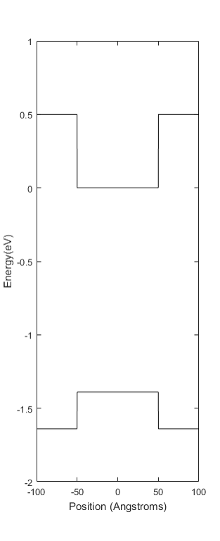
The first step in our model is modeling the potential energy surface of the quantum well. This is visualized in Figure 1, where the band gap of GaAs is set to be about 1.39 eV and the band gap of AlGaAs is set to be 2.14 eV [3]. GaAs/AlGaAs is a Type I heterostructure, where the band gap of the inner semiconductor is between the band gap of the outer semiconductors. Additionally, the difference between the gaps is approximately 66% in the conduction band and 33% in the valence band [5].
Next, we calculate the eigenfunctions and energy levels for the quantum wells, shown in Figure 2. In semiconductors, due to interference effects, the electron behavior in the conduction band is modeled by a particle with an effective mass of .069 e-[5]. The behavior of the electron hole in the valence band is modeled by a heavy hole with an effective mass of .35 e-[5]. This would explain the differences between the energy spacings depicted in the literature between the valence and conduction bands.
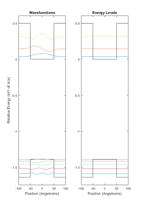
Once we have calculated the relative energy spacings of the conduction and valence bands, we can find the transition energies that would occur in this material. We note that the relevant transitions are those involving the same levels. For instance, the transition between valence energy level 1 and conduction energy level 1. This is because the absorption of energy is proportional to the overlap integral between the wavefunctions.
![Figure 3: Experimental Absorption Peaks [5]](/assets/quantum-wells/Fig3.png)
Based on our model, the three main transitions would occur at 1.4035 eV, 1.4440 eV, 1.5110 eV. When we compare these results to the experimental results shown in Figure 3, it appears that the two are slightly different, but on the same order of magnitude in terms of absolute value and relative spacing. This is likely due to the fact that the exact estimates used in the model for both the band gaps as well as the effective masses and well length may not have matched up to the experimental set up, as these exact details were not described.
Another important difference is that the experimental results show pairs of peaks. This difference is due to the fact that our model does not account for the creation of an exciton in the semiconductor. When an electron absorbs energy and moves from the valence band to the conduction band, it leaves an electron hole. The promoted electron and the electron hole exert a Coulomb force on one another. This bound state is like a Hydrogen atom, which consists of a proton and an electron in a bound state. The exciton itself has energy, about .04 eV, which explains the pairing of absorption peaks in the experimental data [5].
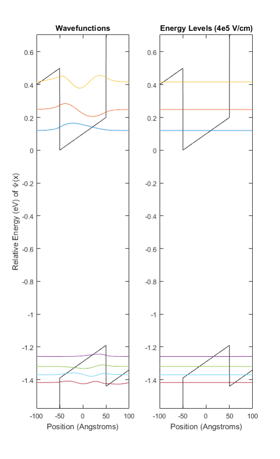
Next, we model the application of a perpendicular electric field to the semiconductor material. This tilts the potential well surface. We see this in Figure 4. We calculate the wavefunctions and the energy levels for this potential surface. The wavefunctions are Airy functions [5].
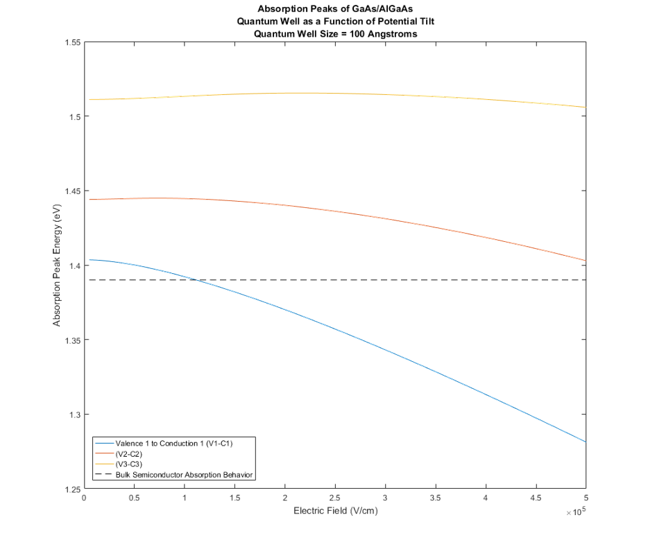
When we graph the same three transitions from earlier as a function of electric field in Figure 5, we see that the transitions shift from higher energies to lower energies as the electric field strength increases. When we compare this to the experimental data, in Figure 6, we see that this result is consistent with the experimental data.
![Figure 6: Experimental Shift in Absorption [5]](/assets/quantum-wells/Fig6.png)
Finally, because we have changed the wavefunctions, we can now witness an increased set of transitions. Recall that the transitions were proportional to the overlap integral. Since the wavefunctions have changed, the overlap integral between different energy levels is now relevant. If we graph the overlap transitions as a function of electric field, we get the graph in Figure 7.
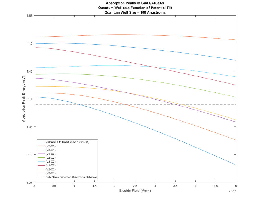
This behavior appears to be similar to the Stark Effect in Hydrogen, which is depicted in Figure 8.
![Figure 8: Stark Effect in Hydrogen [8]](/assets/quantum-wells/Fig8.png)
It is no surprise then that the two are related. Because of physical difficulties of performing experiments on Hydrogen to witness the Stark Effect in Hydrogen, many mechanically analogous experiments may be performed on excitons trapped in quantum wells [5].
Conclusion and Outlook
As discussed in the results section, our simple model of a GaAs/AlGaAs quantum well produces results that are close to but not exactly the results obtained experimentally. While there may a number of reasons why our model differs from the experimental results, at the core, the model seems to be able to account for some of the effects observed experimentally, such as the quantum-confined Stark Effect, which we demonstrated. Because this type of model shows promise, it should be possible to use this model to estimate different potential wells and potential energy surfaces. For instance, a surface created with three different semiconductors, etc.
While quantum wells and the quantum-confined Stark Effect are relatively well understood and researched, the future of optoelectronic devices is still being created through research. This project demonstrates that even basic models, such as those taught in introductory quantum mechanics for chemistry classes, can go a long ways towards understanding very important and very useful real world phenomenon. Indeed, as history has demonstrated, technological advances have relied on a combination of theoretical and physical advances, something the field of semiconductor research fits right into the center of.
References
- Dresselhaus, M. (n.d.). Two Dimensional Electron Gas, Quantum Wells & Semiconductor Superlattices [PDF]. Cambridge: MIT. 6.732 Solid State Physics: http://web.mit.edu/6.732/www/new_part1b.pdf
- Handout 6 Semiconductors and Insulators [PDF]. (n.d.). http://www2.physics.ox.ac.uk/sites/default/files/BandMT_06.pdf
- Kittel, C. (1986). Introduction to solid state physics (6th ed.). New York: Wiley. p. 185
- McGarry, S. (n.d.). Energy Band Diagrams and Doping [PPT]. Ottawa, Ontario: Carleton University. ELEC 3908, Physical Devices – Lecture 3: http://www.doe.carleton.ca/~smcgarry/ELEC3908/Slides/ELEC3908_Lect_3.pdf
- Miller, D. A. (1996). Optical physics of quantum wells. Quantum Dynamics of Simple Systems,” ed. G.-L. Oppo, SM Barnett, E. Riis, and M. Wilkinson (Institute of Physics, London, 1996), 239-26.
- Miller, D. A. B., Chemla, D. S., Damen, T. C., Gossard, A. C., Wiegmann, W., Wood, T. H., & Burrus, C. A. (1984). Band-edge electroabsorption in quantum well structures: the quantum-confined Stark effect. Physical Review Letters, 53(22), 2173.
- Shum, K. (n.d.). Semiconductor quantum wells [PDF]. New York City: City University of New York. http://userhome.brooklyn.cuny.edu/kshum/documents/q1Deigenstates-implementedbyGaAs-AlGaAs.pdf
- Singh, J. (2001). Semiconductor devices: Basic principles. New York: Wiley.
- The Stark Effect. (n.d.). Retrieved December 10, 2016, from http://www.starkeffects.com/stark_effect.shtml
Appendix
find_eigenfunctions.m (Lab 3, PS10, Fall 2016, Harvard University)
function [eigenfunctions,E] = find_eigenfunctions(X,V,mass,hbar,n)

% takes X, a vector of x-coordinates and V, the potential energy at these
% points, and returns the n lowest eigenvalues and their corresponding eigenfunctions.
% mass and hbar are the particles mass and the reduced Planck's constant
% respectively.

% useful numbers
xsize = length(X);
dx = X(2)-X(1);

% create a xsize-by-xsize matrix representing the second derivative
% operation. Note that at the endpoints, X(1) and X(end), the second
% derivative is undefined. Mulitplying by this matrix gives the second
% derivative as it would be if the wavefunction vanished beyond the
% endpoints - effectively imposing vanishing boundary conditions.
d2dx2 = (diag(ones(xsize-1,1),1) + diag(ones(xsize-1,1),-1) - 2*diag(ones(xsize,1),0))/dx^2;


% We create a matrix representing the Hamiltonian, containing both the kinetic
% energy (d2dx2) and the potential energy, V. The function eigs works
% fastest if it is told to find the lowest magnitude eigenvalues. To ensure
% that we don't miss negative eigenvalues, we subtract Vmin from the
% potential to ensure that all the eigenvalues are positive. We then
% subtract this from the eigenvalues at the end.
Vmin = min(V);
Hamiltonian = diag(V-Vmin) - hbar^2/(2*mass)*d2dx2;

% Here is the engine that does all the work for us, it finds the n smallest
% eigenvalues and eigenvectors of the matrix 'Hamiltonian'
[V, D] = eigs(Hamiltonian, n,'sm');

% unfortunately, 'eigs' gives us the eigenvectors and eigenvalues in the
% wrong order and orientation. The next lines just correct for this.
tmp = V(:,n+1-(1:n));
eigenfunctions = tmp'; % this is the output 'eigenfunctions'

tmp2 = diag(D+Vmin); % this turns the diagonal matrix that eigs spits out into a vector
E = tmp2(n+1-(1:n)); % this is the output 'E'
end
find_absorption_peaks.m
function [absorption_peaks] = find_absorption_peaks(size_of_well, number_of_peaks, if_plot)

% Calculates simple absorption peaks for quantum wells of GaAs/AlGaAs
% for a given well length in Angstroms and the number of levels
% find_absorption_peaks(
%   size_of_well: Size of the quantum well in angstroms
%   number_of_peaks: Number of absorption peaks to calculate
%   if_plot: Boolean to indicate whether a plot is desired
% );

% Set some constants for the calculation
num_estates = number_of_peaks;

% Physical parameters
% The units are a method of simplying the final computations
m_0 = 0.057; % of electron in units of eV.Angstrom^-2.fs^2
mass_e = .069 * m_0; % Effective electron mass in quantum well
mass_hh = .35 * m_0; % Effective electron hole mass in quantum well
hbar = 0.66; % eV.fs
bandgap = 1.39; % bandgap of GaAs in eV

% Create a vector of x-positions (x in Angstroms)
range = size_of_well * 2; % Angstroms
dX = range / 1000; % X step size
Xmin = -range;
Xmax =  range;
X = Xmin:dX:Xmax;
xsize = length(X);

% The conduction band calculations
% GaAs / AlGaAs is a "Type I" heterostructure
% The energy difference between GaAs and AlAs is split 66/33 between
% the conduction band and the valence band. We have set this difference to
% be about .75 eV based on estimates of the semiconductor band gaps
energy_of_walls = .5; % eV
% Create the potential well for the conduction band
V_1 = repmat(energy_of_walls,1,500);
V_2 = zeros(1,1001);
V_3 = repmat(energy_of_walls,1,500);
V = [V_1, V_2, V_3];

% Find the energy levels and also the eigenfunctions
[EFunc,E] = find_eigenfunctions(X,V,mass_e,hbar,num_estates);

% These are the calculated values of the conduction band
conduction_potential = V;
conduction_energies = repmat(E,1,xsize);
conduction_E = E;
conduction_wavefunctions = -1 * EFunc + repmat(E,1,xsize);

% The valence band potentials
energy_of_walls = .25; % eV
V_1 = repmat(energy_of_walls,1,500);
V_2 = zeros(1,1001);
V_3 = repmat(energy_of_walls,1,500);
V = [V_1, V_2, V_3];

% Find the energy levels and also the eigenfunctions
[EFunc,E] = find_eigenfunctions(X,V,mass_hh,hbar,num_estates);

% These are the calculated values of the valence band
valence_potential = -V - bandgap;
valence_E = -E - bandgap;
valence_energies = -repmat(E,1,xsize) - bandgap;
valence_wavefunctions = -(.25 * EFunc + repmat(E,1,xsize)) - bandgap;

if if_plot
    % Plot the energy levels
    figure(1)
    plot(X, conduction_potential,'k',...
        X, conduction_energies);
    hold on;
    plot(X, valence_potential,'k',...
        X, valence_energies);
    % A little hacky here
    ylim([min(valence_wavefunctions(:)) - .05, max(conduction_wavefunctions(:)) + .15]);
    xlim([-range * .8, range * .8]);
    xlabel('Position (Angstroms)');
    ylabel('Energy (eV)');
end

% Get the values of the energy of absorption peaks
absorption_peaks = conduction_E - valence_E;
end
find_stark_absorption.m
function [absorption_peaks] = find_stark_absorption(size_of_well, number_of_peaks, if_plot, slope)

% Calculates simple absorption peaks for quantum wells of GaAs/AlGaAs
% for a given well length in Angstroms and the number of levels
% find_absorption_peaks(
%   size_of_well: Size of the quantum well in angstroms
%   number_of_peaks: Number of absorption peaks to calculate
%   if_plot: Boolean to indicate whether a plot is desired
%   slope: Slope of the electric potential of the quantum wells
% );

% Set some constants for the calculation
num_estates = number_of_peaks;

% Physical parameters
% The units are a method of simplying the final computations
m_0 = 0.057; % of electron in units of eV.Angstrom^-2.fs^2
mass_e = .069 * m_0; % Effective electron mass in quantum well
mass_hh = .35 * m_0; % Effective electron hole mass in quantum well
hbar = 0.66; % eV.fs
bandgap = 1.39; % bandgap of GaAs in eV

% Create a vector of x-positions (x in Angstroms)
range = size_of_well * 2; % Angstroms
dX = range / 1000; % X step size
Xmin = -range;
Xmax =  range;
X = Xmin:dX:Xmax;
xsize = length(X);

% The conduction band calculations
% GaAs / AlGaAs is a "Type I" heterostructure
% The energy difference between GaAs and AlAs is split 66/33 between
% the conduction band and the valence band. We have set this difference to
% be about .75 eV based on estimates of the semiconductor band gaps
energy_of_walls = .5; % eV
% Create the potential well for the conduction band
V_1 = repmat(energy_of_walls,1,500);
V_2 = zeros(1,1001);
V_3 = repmat(energy_of_walls,1,500);
V = [V_1, V_2, V_3];
V = V + ((1:2001) ./ (2001 / slope));
V = V - min(V);

% Find the energy levels and also the eigenfunctions
[EFunc,E] = find_eigenfunctions(X,V,mass_e,hbar,num_estates);

% These are the calculated values of the conduction band
conduction_potential = V;
conduction_energies = repmat(E,1,xsize);
conduction_E = E;
conduction_wavefunctions = -1 * EFunc + repmat(E,1,xsize);

% The valence band potentials
energy_of_walls = .25; % eV
V_1 = repmat(energy_of_walls,1,500);
V_2 = zeros(1,1001);
V_3 = repmat(energy_of_walls,1,500);
V = [V_1, V_2, V_3];
V = V + ((2001 / slope) - ((1:2001) ./ (2001 / slope)));
V = V - V(501);

% Find the energy levels and also the eigenfunctions
[EFunc,E] = find_eigenfunctions(X,V,mass_hh,hbar,num_estates);

% These are the calculated values of the valence band
valence_potential = -V - bandgap;
valence_E = -E - bandgap;
valence_energies = -repmat(E,1,xsize) - bandgap;
valence_wavefunctions = -(.25 * EFunc + repmat(E,1,xsize)) - bandgap;

if if_plot
    % Plot the energy levels
    figure(1)
    plot(X, conduction_potential,'k',...
        X, conduction_energies);
    hold on;
    plot(X, valence_potential,'k',...
        X, valence_energies);
    % A little hacky here
    % ylim([min(valence_wavefunctions(:)) - .05, max(conduction_wavefunctions(:)) + .15]);
    % xlim([-range * .8, range * .8]);
    xlabel('Position (Angstroms)');
    ylabel('Energy (eV)');
end

% Get the values of the energy of absorption peaks
absorption_peaks = conduction_E - valence_E;
end